Our research group focuses on applying/developing varied advanced transmission electron microscopy techniques (HADDF, HREM, EELS, EDS, Lorentz TEM, electron holography, electron tomography, in situ TEM and so on) to determine the nanostructures/atomic structure of materials (mainly energy materials), thus providing insight into observed physical properties. This is of particular importance as electronic devices scale to ever vanishingly small dimensions, when the detailed arrangement of atoms at interfaces even inside materials begins to critically influence material properties. We focus on three areas: Nanostructured energy materials including the nanostructure of thermoelectrics, photovoltaics, fuel cells and batteries, and their real-time evolution during operation; Phase separation in strongly correlated electron systems; Interfacial structures.Our research group focuses on applying/developing varied advanced transmission electron microscopy techniques (HADDF, HREM, EELS, EDS, Lorentz TEM, electron holography, electron tomography, in situ TEM and so on) to determine the nanostructures/atomic structure of materials (mainly energy materials), thus providing insight into observed physical properties. This is of particular importance as electronic devices scale to ever vanishingly small dimensions, when the detailed arrangement of atoms at interfaces even inside materials begins to critically influence material properties. We focus on three areas: Nanostructured energy materials including the nanostructure of thermoelectrics, photovoltaics, fuel cells and batteries, and their real-time evolution during operation; Phase separation in strongly correlated electron systems; Interfacial structures.
-
Thermoelectric materials ————
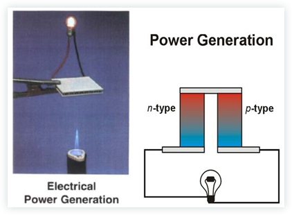
Thermoelectric materials are among the important potential candidates for alternative and complementary sources for energy, wherein heat can be directly converted into electrical energy and vice versa. (Figure 1) These materials are realistic operational materials for applications in thermoelectric generators and refrigerators provided that they have, on average, a figure of merit, ZT, above ~ 2. The figure of merit is defined as ZT = S2\sigma T/\Kappa, where S, \sigma,/\Kappa,T and S2 \sigma are the Seebeck coefficient, electrical conductivity, thermal conductivity, absolute temperature and power factor, respectively.
With the aim of improving the efficiency of thermoelectric energy conversion, many efforts to increase ZT have focused on increasing the Seebeck coefficient and electrical conductivity, while reducing thermal conductivity,kappa, which is the sum of the lattice-,Kappa lat, and the electronic-, Kappa lat ele, contributions. Each parameter quantifies the heat-carrying efficiency of phonons for a given lattice, and of charge carriers, respectively. However, the challenge is to minimize thermal conductivity while retaining desirable electronic transport properties. Some researchers have developed new ways to introduce nanostructures into the thermoelectric matrix, which results in much higher phonon scattering and thus lower lattice thermal conductivity. Many synthetic techniques have been proposed to insert these nanostructures; such as the fabrication of superlattices or quantum dots, nanocrystalline inclusions, and self-organization, as well as formulating new structures. Despite the formulation of numerous methods to reduce thermal conductivity and sustain electrical conductivity, the underlying mechanisms are poorly understood which can be done by TEM.

-
CMR materials ————

Manganese oxides have attracted great scientific interest due to their unusual electronic transport and magnetic properties, such as CMR and spin-, charge-, and orbit- ordering. The CMR property is known to be related to the ferromagnetic metallic state. Magnetic domains and domains walls in the ferromagnetic phase may not only strongly affect magnetic properties but also the electron-transport properties of these oxides. The reversal of magnetization at a domain wall in an uninterrupted CMR perovskite crystal does not significantly scatter the charge carriers. The highly localized Mn3/2 spins are expected to form wide domain walls, such that strong on-site Hund interactions do not prevent the itinerant spins from adiabatically tracking the magnetic twist. We consider that a precise analysis of magnetic microstructure is of vital importance both for our fundamental understanding of these phenomena, and for applications of advanced magnetic materials.
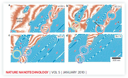
Magnetic-domain structures, charge-ordered phase, and phase separation (Figure2) of CMR thin film could be investigated by Lorentz electron microscopy.
-
Ferroelectric materials ————
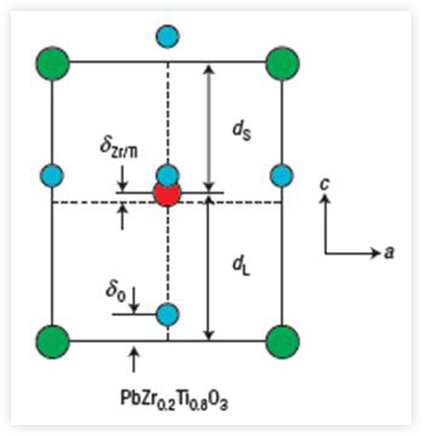
Epitaxial ultrathin (a few nanometres thick) films of ferroelectric oxides, such as Pb(Zr,Ti)O3 (PZT), BaTiO3 (BTO) and Ba1-xSrxTiO3(BST), have attracted considerable attention with respect to potential applications in nanoelectronic high-density memory devices. The magnitude and stability of the switchable ferroelectric polarization are the central figures of merit for such devices. How the polarization scales with reduced thickness, particularly when the film thickness becomes smaller than typically 10 nm, is now an intensely debated topic. This so-called size effect represents one of the most intriguing phenomena in the area of thin-film ferroelectrics.
For examples, in ultrathin epitaxial PbTiO3 (PTO) films deposited on conducting Nb-doped SrTiO3 (STO) substrates, the decrease in measured polarization is commensurate with a corresponding decrease in the tetragonality and is in line with the traditionally accepted model of a strong strain-polarization coupling in such systems. On the other hand, studies on ultrathin PTO films on SrRuO3 (SRO)-buffered STO did not show a decrease in the out-of-plane lattice parameter measured at room temperature. This has been considered as evidence for the fact that the electrical boundary conditions play a very important role in the stabilization of the ferroelectric polarization for films with a thickness of a few lattice unit cells.
As well known, interface-related issues have been identified. These are: a time-dependent decay in the switchable polarization resulting from a non-zero depolarization field at the interface, sharing of the ionic displacements by the electrode or substrate and severe constraints imposed by the electrode-ferroelectric interface. To further complicate the matter, leakage currents can strongly influence the results of polarization measurements and it is a formidable task to separate leakage effects from intrinsic polarization switching currents when carrying out polarization measurements on such ultrathin systems. Also the measured decay of the switchable polarization in ultrathin films is strongly dependent on the materials system and to date no consistent explanation has been found for the large variety of experimental results

-
Superconductivity materials ————

The epitaxial growth of La2-xSrxCuO4 (LSCO) superconductor films has attracted much attention because of the remarkable effects of epitaxial strain on their critical temperature, Tc. Basically, substrates create two types of in-plane strain on the films: compressive strain if the film's lattice constant, af, is greater than that of the substrate, as; and, tensile strain if af < as. Usually, the in-plane compressive strain raises Tc, while the in-plane tensile strain lowers it. However, what is most relevant is that the residual strain strongly depends on the lattice mismatch between the film and the substrate. The state of strain in a film can differ considerably from that found in bulk materials in reference to the configuration of microstructure and lattice defects. Similarly, the electrical properties (e.g., Tc) of a strained film can differ from those in the bulk. The lattice mismatch between a thin film and its substrate is one important parameter that greatly influences the film's structure, morphology, and its remaining strain. The energy stored within an epitaxial film due to the lattice-misfit strain increases with the film's thickness, which is a second determining factor. Thus, at a certain critical thickness, tcr, dislocations form at or near the substrate/film interface as it becomes energetically favorable to relieve the strain. Two other independent variables usually affecting the configuration of the defects and the residual strain are the particular substrate chosen, and the processing conditions employed.
LSCO is antiferromagnetic layered perovskite oxide. When LSCO films are grown on STO bicrystal substrates, their microstructure, chemical composition, and spin state around the boundary changes. Our work will monitor the alterations in atomic structure (by STEM), in chemical structure (by EELS), and in spin structure (by electron holography). The challenges of this work are that we need high-quality TEM samples (assured by careful preparation), and high-resolution images from STEM, EELS, and electron holography.
We will investigate the atomic-, chemical-, and spin-structures of LSCO thin films grown on SrTiO3 (STO) bicrystals by STEM, EELS, and electron holography.


